Sony Announces The World's First Dual-Light-Sensitive 'Stacked CMOS' Sensor
A pioneer in digital imaging, Sony announced its first stacked CMOS sensors for full-frame cameras back in April 2017 on the flagship Sony A9 camera. A stacked CMOS sensor captures significantly more exposure, offers faster frame rates, and better image processing. Now, Sony's Semiconductor unit has announced the world's first stacked CMOS sensor with dual transistor layers that doubles the amount of light captured in comparison to a conventional stacked sensor.
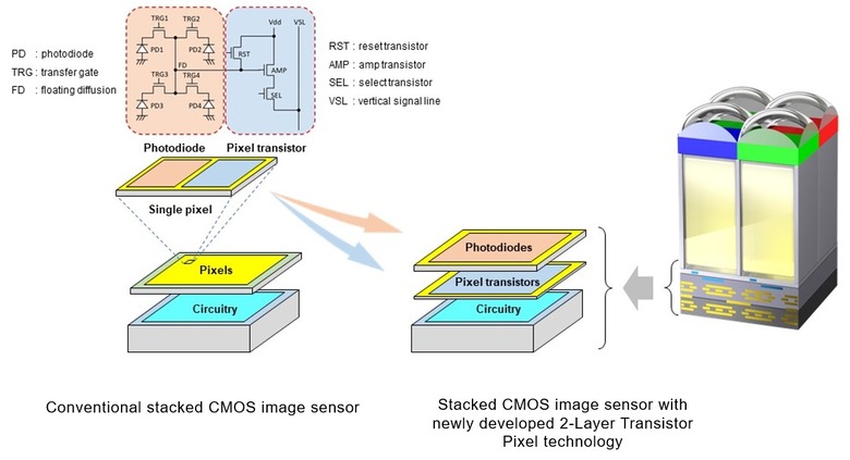
Sony says that while a traditional stacked CMOS sensor has pixel transistors and photodiodes on the same substrate layer, the new dual-layer arrangement places them in two different substrate levels. This structure basically allows the sensor to capture twice the saturation signal level, and thus, improves the dynamic range of the images as well as the noise reduction.
Precise saturation tracking on Sony's 2-layer stacked CMOS sensor
Sony Semiconductor Solutions Corporation, Japan
Although higher saturation signal levels do not directly correspond to better exposure capturing, the characteristic does come in handy when the sensor is trying to detect illumination, especially in dark ambiances. Therefore, doubling the saturation signal gain will not translate into twice the exposure level but, it will definitely imply an improvement.
Sony is confident the new technology widens the "dynamic range and noise reduction available from this new technology will prevent underexposure and overexposure in settings with a combination of bright and dim illumination (e.g., backlit settings) and enable high-quality, low-noise images even in low-light (e.g., indoor, nighttime) settings."
The Japanese giant labels this new two-layer arrangement as an "advancement" over the standard stacked CMOS sensor. Photodiodes, which convert light into electric signals, and pixel transistors, which control these signals, are located side-by-side on the same flat plane in a typical stacked sensor. By using two different layers of substrates, each of the layers can be individually optimized to improve the uptake of light.
Sony also says the separation of transfer gates from other transistors will make room for bigger signal amplifiers (aka amp transistors), and this increase, in turn, can be utilized to limit noise in images captured in dim environments.
Sony teases 2-Layer CMOS sensors for smartphones
Sony also says it will soon implement high-quality imaging on other devices including smartphone cameras with this two-layer transistor pixel technology. This means, we can very well expect much better cameras on all smartphones using Sony IMX sensors — not just its own Xperia series, even though the latter could benefit from some premium features.
Lastly, Sony does not announce when this technology could make its way to commercial devices but we hope to not just hear about but also experience advancements in this area very soon.


