Sony VAIO X Teardown Reveals Huge Engineering Ingenuity
While we always enjoy the post-launch teardown photosets that spring up following a particularly noteworthy piece of hardware, sometimes we wish there was an engineer to hand to tell us whether what we're looking at really is all that impressive. TechOn did just that with Sony's indecently-skinny VAIO X, in a seven part hands-on and teardown that pits an unnamed engineer – who, from the sound of it, works for a rival OEM – against Sony's ingenuity. In case you hadn't guessed, the VAIO X really is a masterpiece of manufacturing.
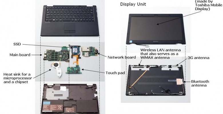
For instance, the display panel doesn't route the antennas around the edge, as many bulkier notebooks do, but sandwiches LCD and antenna array together in two flat sheets. Sony have seemingly reduced a standard 0.37mm thick glass plate down to sub-0.21mm thickness by grinding it. Meanwhile all the mainboard components are mounted on one side, including some ports that appear to be hand-soldered into place; that's meant that Sony needed to reduce the number of capacitors and other components in order to squeeze them in.
"Of all the features of the VAIO X, I was most impressed by the fact all the components are mounted on one side. It is necessary to reduce the number of components to realize such a design. Also, patterning is much easier when components are mounted on both sides" unnamed engineer, TechOn
The end result is a machine that the engineer reckons would have cost twice as much to manufacturer as a regular notebook, and demanded comprehensive cooperation between the designers, engineers and production plants from early on in the project. The VAIO X may be hugely expensive and underpowered, but it's certainly an engineering marvel.
"I felt that Sony put its whole heart into developing this. I would like to have a drink with the designers of the VAIO X. I think I will find a kindred spirit in those people" unnamed engineer, TechOn
