SK Hynix Shows Off 176-Layer 4D NAND Flash
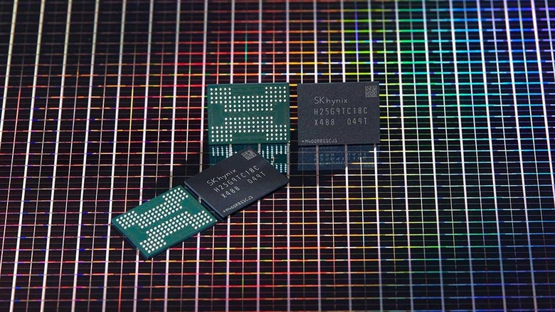
SK hynix has announced that it has completed the development of the industry's most multilayered 512-gigabit triple-level cell (TLC) 4D NAND flash comprised of 176 layers. The company says it provided samples to controller companies last month so they could design products around it. Previously, SK hynix promoted its 4D technology using a 96-layer NAND flash product combining Charge Trap Flash with high-integrated Peri.
The new 176-layer NAND flash is a third-generation 4D product the company says secures the industry's best number of chips per wafer. More chips per wafer allows bit productivity to be improved by 35 percent compared to the prior generation with differentiated cost competitiveness. Cell read speed is improved by 20 percent over the past generation by adopting two-division cell array selection technology.
SK hynix has also increased data transfer speed by 33 percent to 1.6 Gbps by adopting speed-up technology without increasing the number of processes. Consumer and enterprise SSDs using the new technology will be available by the middle of next year with 70 percent higher maximum read speed and 35 percent higher maximum write speed.
SK hynix says it overcame challenges posed by increasing the numbers of layers in a NAND flash product, such as the cell current reduction, channel twisting, and cell distribution deterioration due to doublestack misalignment. It overcame those obstacles using cell interlayer height reduction, layer variable timing control, and ultra-precise alignment.
Among the products that will be developed using the new 176-layer NAND flash are 1Tb products with double density using the new NAND. Faster read and write speeds are always welcome in storage products, and this is good news for enterprise users and computer enthusiasts. There is no indication of how much products might cost that use the new technology.