NVIDIA Details 22-Day Process Of Developing The Tegra 4i
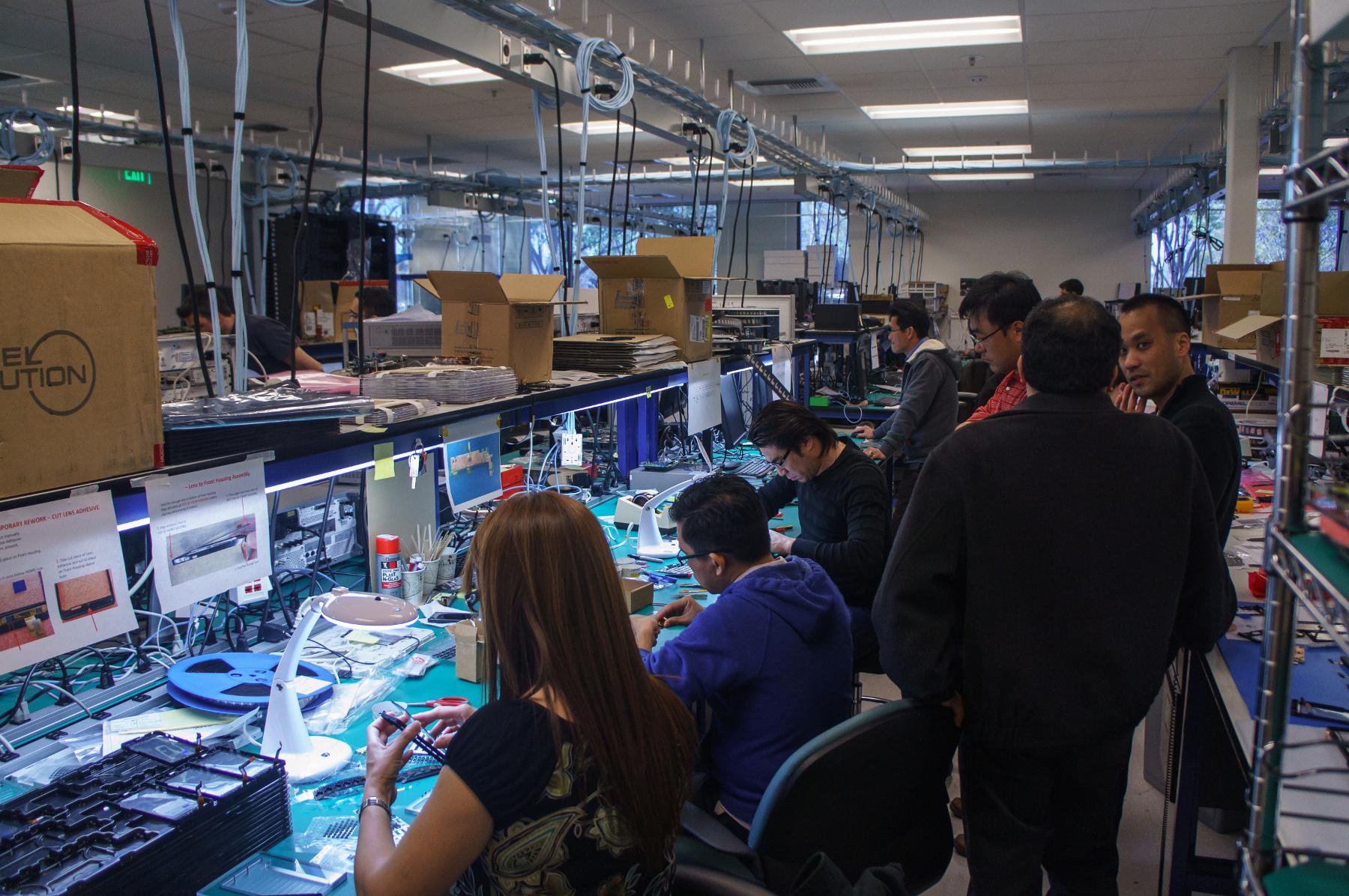
The NVIDIA team worked long and hard to ensure that the NVIDIA Tegra 4i would be ready to show off by the time Mobile World Congress came around. The team worked non-stop from February 3rd (the day of Super Bowl) to February 25th, the first day of MWC. The entire 22-day process was exhausting, but the NVIDIA team pulled through and was able to bring their next-gen mobile processor into the world.
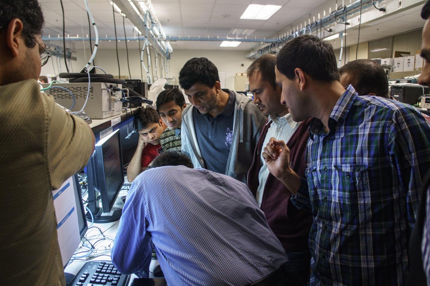
The NVIDIA Tegra 4i is NVIDIA's first mobile processor with an integrated modem. The modem would allow NVIDIA to bring next-gen wireless networking into the smartphone market. Over 200 engineers got straight to work once their package of new silicon chips arrived at SFO from Taiwan. These engineers sacrificed their social lives and sleep in order to develop their next-gen product.
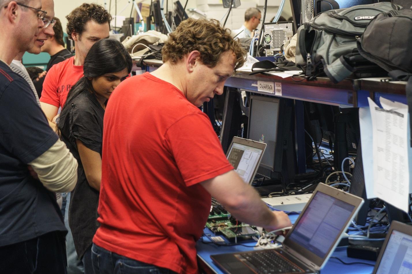
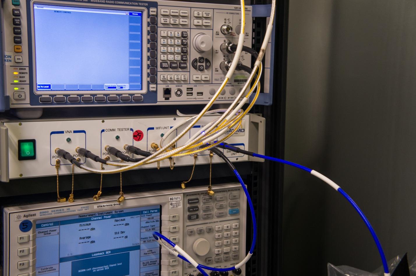
The engineers came from all parts of the world. They worked diligently on testing out new features, stressing each component, working on the upfront designs of each part, and transforming this all into a working product. NVIDIA dubbed this process, "bringup". They spent nearly 24 hours a day working on the chip, and saw all their hard work come to life when the chip booted into Android and successfully sent a message to NVIDIA's CEO.
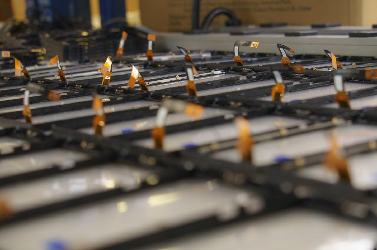
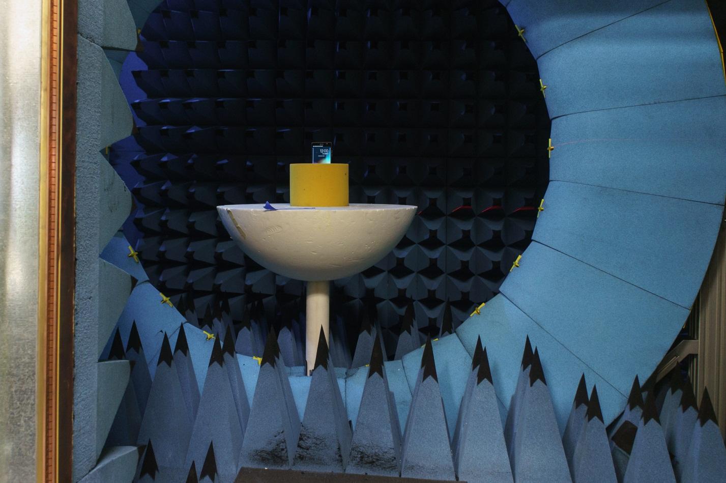
After successfully testing out the chip, NVIDIA's system engineering team worked on developing several Phoenix model phones to show off the chip's capabilities. By the time MWC rolled around, NVIDIA was able to show off the Phoenix model phone that was more than just a phone showing off a display loop. It was instead a full-featured phone that could be used and tested by the public. Be sure to check out our detailed review of the NVIDIA Tegra 4i to see what the NVIDIA team was able to develop. Also be sure to check out our Tegra Hub for the latest information in Tegra news.
[via NVIDIA]
