MIT Researchers Developed A New Method Of Making Graphene Sheets
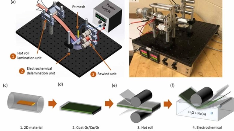
Researchers at MIT have developed a new way of making large sheets of high-quality, atomically thin graphene. Researchers believe that the new manufacturing method could lead to ultra-lightweight, flexible solar cells, and two new classes of light-emitting devices and other thin-film electronics. The process is reportedly relatively easy to scale up for industrial production.The process involves an intermediate "buffer" layer of material that is key to the success of the manufacturing technique. The buffer allows the ultrathin graphene sheet to be less than a nanometer thick and to be easily lifted off its substrate allowing for rapid roll-to-roll manufacturing. Scientists have worked hard to discover a way to make thin, large-area, transparent electrodes that are stable in the open air.
Such a material can be used in a variety of applications in optoelectronic devices like computer and smartphone screens or other devices. One big benefit of graphene is that it's a form of pure carbon with atoms arranged in a flat hexagonal array with good electrical and mechanical properties. The material is very thin and physically flexible, with construction from an abundant and inexpensive material.
The material is easy to grow in large sheets using chemical vapor deposition using copper as a seed layer. The trickiest part has been finding ways to release the graphene from its native copper substrate. The new technology MIT researchers developed allows for reliable manufacturing of large-area graphene sheets.
The key is reportedly a buffer layer made of a polymer called parylene that conforms at the atomic level to the graphene sheets on which it is deployed. Parylene is produced using chemical vapor deposition, which simplifies the manufacturing process and scalability. Aim prototyped graphene-based solar cell improved the delivered power per weight by roughly 36 times while using 1/200 the amount of material per unit area for the transparent electrode.