Samsung's 3D Memory Package
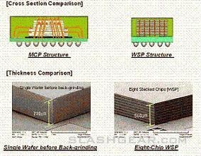
Samsung' industry-first WSP is a 16Gbit memory solution that stacks eight 2Gb NAND chips. The WSP generates a much smaller multi-chip package (MCP), which is the current mainstream solution for designing miniaturized, high-capacity memory devices. Samsung's eight-chip WSP prototype sample, which vertically stacks eight 50㎛ (micrometers), 2Gb NAND flash die, is 0.56 millimeters in height.The chips in today's MCPs are connected by wire bonding, which requires vertical gaps between dies that are tens of microns wide and horizontal spaces on the package board that are hundreds of microns wide to accommodate the wire connections. By contrast, WSP forms micron-sized holes that penetrate through the silicon vertically to connect circuits directly, eliminating the need for gaps of extra space and wires protruding beyond the sides of the die. Due to these advantages, WSP has a 15-percent smaller footprint and is 30 percent thinner than an equivalent wire-bonded MCP solution.