Samsung 7nm EUV chip production gets underway
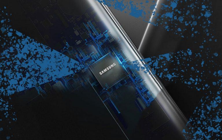
Samsung Electronics revealed they'd gotten underway with wafer production on its next process node, 7nm LPP EUV. That's also known as 7-nanometer (nm) LPP (Low Power Plus) with extreme ultraviolet (EUV) lithography technology. Also in the mix this week were new SmartSSD, QLC-SSD, and 256GB 3DS RDIMM.
Samsung revealed the production at their Samsung Tech Day alongside several other innovations and milestones in processing products. The big deal here is the fact that 7nm production is underway – but the underlying greatness is in the tech itself. Samsung's 7nm LPP EUV represents significant strides past the most recent generation in 10nm processes.
Samsung 7nm LPP EUV vs 10nm processes
• Maximum of 40% area reduction
• 50% dynamic power reduction
• 20% performance increase
Applications listed as potential boundary-pushers that'll use this 7nm process were as follows: 5G (data connectivity), Artificial Intelligence (AI), Enterprise and Hyperscale Datacenters, IoT projects of all sorts, Smart Automotive, and of course the always-present Networking.
"This fundamental shift in how wafers are manufactured gives our customers the opportunity to significantly improve their products' time to market with superior throughput, reduced layers, and better yields," said Charlie Bae, executive vice president of foundry sales and marketing team at Samsung Electronics. "We're confident that 7LPP will be an optimal choice not only for mobile and HPC, but also for a wide range of cutting-edge applications."
With an announcement of production of 7LPP, Samsung also made clear the current Samsung Foundry tech roadmap, providing users with "a definite path to 3nm."
Also revealed at Samsung Tech Day were SmartSSD, a new 1Tb QLC-SSD, and the impressive 256-gigabyte (GB) 3DS (3-dimensional stacking) RDIMM (registered dual in-line memory module). SmartSSD will incorporate an FPGA accelerator into the SSD unit, resulting in bypassed server CPU limits and faster data processing. Also as a result of said incorporation, says Samsung, users will see "higher processing performance, improved time-to-insight, more virtual machines (VM), scalable performance, better de-duplication and compression, lower power usage and fewer CPUs per system."
Samsung aimed to further break performance barriers with a 1Tb QLC-SSD, Z-SSD and 8GB Aquabolt. Said a Samsung representative, "The 8GB Aquabolt provides the fastest data transmission speed and highest performance of any DRAM-based memory solution on the market today at 307GB/s per HBM cube." Samsung also suggested that systems with their tiered solution of QLC-SSD and Z-SSD "results in a 53-percent increase in overall system performance." Seems like a pretty beefy claim – we'll see!