MIT engineers create 3D transistors half the width of the smallest transistors available today
MIT has announced an engineering breakthrough that has resulted in the smallest 3D transistors ever created. These new MIT transistors are half the width of the slimmest commercial models available today. MIT worked with the University of Colorado on this new transistor.
To create the tiny transistor the scientists had to create a new microfabrication technique to modify the semiconductor material atom-by-atom. The team says that the inspiration for their work was the desire to keep up with Moore's Law, which was an observation made in the '60s that the number of transistors on an integrated circuit doubles about every two years.
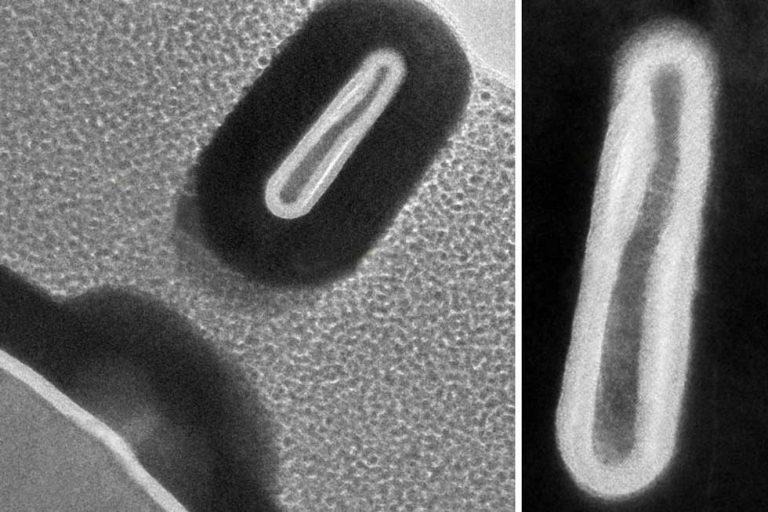
Chipmakers have had a difficult time sticking with Moore's Law in recent times as it is getting more challenging to keep doubling the number of transistors using current technology. The 3D transistors stand vertically like fins and are about 7nm across. That is tens of thousands of times thinner than a human hair.
These new transistors are so small that tens of billions of them can fit on a single microchip about the size of a fingernail. The creation of the new transistors was enabled using a newly invented chemical-etching technique called thermal atomic-level etching or thermal ALE. The method can precisely modify semiconductor materials at the atomic level.
That technique has been used to create transistors as narrow as 2.5-nanometers that are also more efficient than commercially available options of today. Researchers say that while similar atomic-level etching methods do exist today, the new technique is more precise and yields higher-quality transistors. The new technology also uses a common microfabrication tool used for depositing atomic layers on materials allowing it to be rapidly integrated into assembly lines.