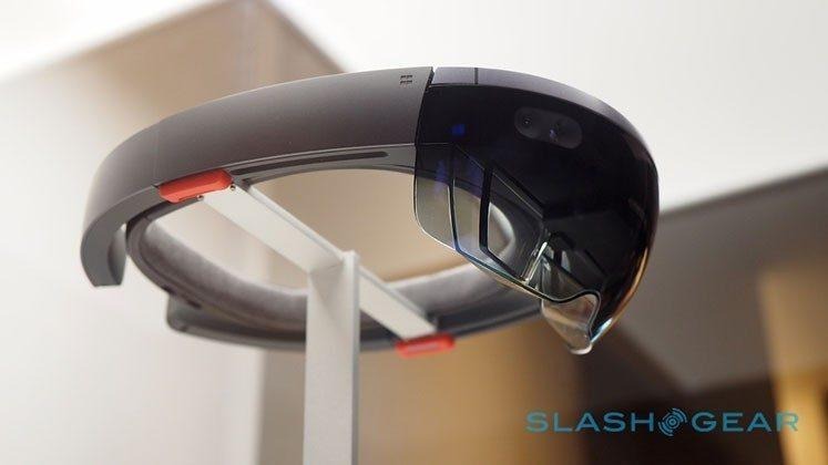
Microsoft HoloLens powered by TSMC holographic processing unit
If there were questions as to why AR headsets like Microsoft's HoloLens are so expensive and so rare, then this little tidbit might explain things a bit. Although it was already revealed that the headset uses an Intel Atom Cherry Trail for its main processor, that isn't actually the one doing the heavy lifting. Instead, it is the 28 nm "holographic processing unit" or HPU fabricated by TSMC that does most of the sensor processing required to deliver a fluid, real-time AR experience.
That HPU is quite remarkable in many ways. It utilizes 24, yes 24, Tensilica DSP cores, or Digital Signal Processing, for taking all the data thrown at it by sensors and processing them. All of that happens on hardware so that it's super fast, as much as a trillion calculations per second. The HPU custom designed for that kind of processing so that it is actually faster doing it on this kind of processor than passing it on to the Intel x86 CPU.
The HPU has 8 MB of SRAM and its own 1 GB of LPDDR3 RAM, separate from than it the Atom CPU's own 1 GB RAM. The chip draws less than 10 w of power, which is remarkable power sipping considering all the processing that it does. By the time the data reaches the Intel CPU, it has mostly been processed already so that the CPU has less to do. It's almost like how motion sensor data processing on some smartphones, like the iPhone, are offloaded to a dedicated low-power chip to keep the more power-hungry CPU running as seldom as possible.

Microsoft has added custom instructions to the HPU, making it a very customized component. As such, it is far from something that can be easily commoditized. We are, however, still at the earliest days of augmented, really mixed, reality, and hopefully, in the future, such hardware will be more common in order to make AR headsets like the HoloLens also more common.
VIA: The Register