iPhone 5s A7 chip teardown gets transistor-deep
The teardown of the iPhone 5s has officially gotten microscopic. With the team at chipworks making it their mission to get down and dirty with the heartiest Apple chip on the market today, the iPhone 5s has joined the ranks of the devices that our current teardown culture has seen fit to take apart down to the tiniest of details. Tearing the top off the processor as you'd see it first when you pop off the back of the iPhone 5s (not recommended, by the way,) a new conglomeration is revealed.
Under the hood you'll find chipworks laying out what they feel is an accurate floorplan for the Apple A7 chip, including about 17% of the die being dedicated to the dual-core CPU. After this you'll find a large portion of the architecture appearing to be taken up by the GPU. Graphics finesse is a definite must when you've got always-on moving wallpapers, after all.

There's a bit more information on the architecture as far as the 32nm A6 chip from previous generation iPhones go as they relate to the A7 as well. It's suggested that the 28 nm 6T SRAM cell in this A7 chip is set at around ~0.12 µm2, this compared to the A6's 6 transistor SRAM cell area coming in at ~0.15µm2. It's also suggested that the GPU is a four-cluster iteration of the Imagination-made PowerVR Series 6 known as the G6430 – this information comes from Anand (from AnandTech) who has been working with chipworks on this analysis.
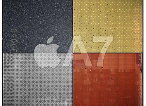
The four-part image you're seeing in this article is an amalgamation of layers in the A7 chip. The black layer is the top – this is the layer you'd see if you somehow pried the back off your iPhone 5s. The gold is the top metal of the architecture, the silver is the x-ray package top, and the red is the guts – that's where the "magic" happens. Be sure to have a peek at SlashGear's iPhone 5s review for more information on what this chip is actually capable of.